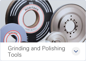
Grinding and Polishing Tools
-
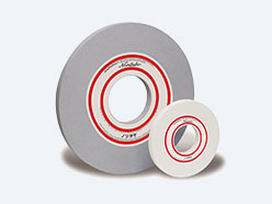
Grinding Wheels
Grinding Wheels
Tools for grinding, polishing and machining various materials.
- Vitrified
- Resinoid
Close
-
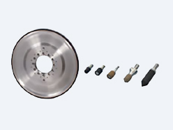
CBN Wheels
CBN Wheels
High-performance, long-life tools using CBN grain.
- CBN Wheels
-
- Crank Shaft Grinding CBN Wheel "Σ Wheel"
- New Porous CBN "FP Wheel"
- Multi-pore General-use CBN Wheel "KP-MEMOX"
- High-precision Flat Lapping CBN Wheel
- Super Long Life Vit-CBN Wheel "MEGA-LIFE WHEEL"
- Mirror-finish CBN Wheel
- Vitrified-bond CBN "Muscle Wheel"
- Centerless Vitrified-bond CBN/Diamond Wheel "Seamless Centerless Wheel"
- Internal Grinding CBN Wheel "XAP Wheel"
Close
-
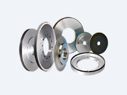
Diamond Tools
Diamond Tools
Tools for machining various non-ferrous materials using diamonds.
- Diamond Tools
-
- Beveling Wheel for Wafer
- Metal Wheel for Super-Hard Main Groove Grinding "Dress-less Metal (MDL)"
- Fixed Diamond Lapping Manufacture Metal Wheel
- Grain Single-layered Metal Bonded CBN Wheel "CBN Grit Ace"
- Honing Wheel Applicable to Water Soluble Coolant
- Grinding Wheel for Super-Hard Drill and Endmill Grinding "i-Flute"
- Cutting Tip Outer Edge Grinding Resin Wheel "i-Surface"
- Resin Bond Wheel for High Quality Profile Grinding "Keep Bright"
- Metal Bond Wheel for High Accuracy Profile Grinding "Keep Edge"
- General-use Multi-pore Diamond Grinding Wheel "SD MEMOX"
- Poreless Vitrified Diamond PCD Grinding Wheel "Smooth Fine"
- Surface Grinding Wheel for Silicon Ingots
- Porous Vitrified-bonded Diamond Wheel "VDH Wheel"
- Vitrified-bond Wheel for Cutting Tip Outer Edge Grinding "VTS Wheel"
- Mirror Finish Resinoid Wheel "Shine-G"
- Diamond dresser
Close
-
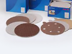
Coated Abrasive
Coated Abrasive
Grinding and polishing tools using grain-coated substrates such as paper and cloth.
- Coated Abrasive
Close
-
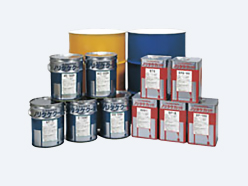
Coolants
Coolants
When grinding, polishing or cutting, Noritake’s coolants will draw out the machining performance of your tools.
- Coolants
Close
-
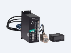
Related Products
Related Products
Noritake offers products for grinding and polishing.
- Related equipment
- Non-slip tape
- Other
Close
-

Grinding & Polishing
Ceramics & Materials
-
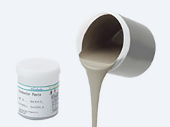
Electronic Paste (Thick Film)
-
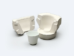
Gypsum
-

Engineering Ceramics
-
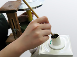
Decoration Materials
-
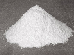
Electronic Ceramic Powder
Electronic Ceramic Powder
Raw materials for use with pottery and glass or electronics field ceramics, etc.
- Electronic Ceramic Powder
Close
-
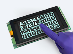
Vacuum Fluorescent Display
Vacuum Fluorescent Display
Displays such as vacuum fluorescent displays and digital signage.
- Vacuum Fluorescent Display
Close
-
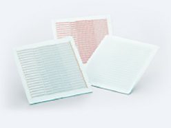
Thick Film Circuit Substrate
Thick Film Circuit Substrate
Highly heat-tolerant circuit substrate made from a ceramic substrate.
- Thick Film Circuit Substrate
Close
Engineering
-
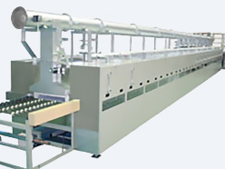
Heating Furnaces / Kilns
Heating Furnaces / Kilns
Heating systems and ancillary products for firing kilns and drying furnaces, etc.
- Heating Furnaces / Kilns
Close
-
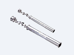
Mixing Technology
Mixing Technology
Noritake provides actuator-less line mixers and related equipment.
- Mixing Technology
Close
-
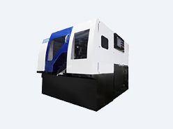
Cutting Machine (Thin Cut Master : TCM)
Cutting Machine (Thin Cut Master : TCM)
Steel and automotive industry-centered machines for cutting and grinding.
- Cutting Machine (Thin Cut Master : TCM)
Close
-
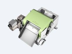
Filtration Systems
Filtration Systems
Industrial filtration systems as well as filtration-related systems are available.
- Filtration Systems
Close


